Reprogrammable NES cartridge
ContentsOverview
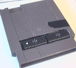 I own a NES (Nintendo Entertainment System) which is in very good shape. Unfortunately, I dont own many games, and some games are very hard to find (eg: Bubble Bubble).
I decided to hack a cartridge to be able to reload it with the software of my choice, which may be a game, a demo, a home-made game, or maybe someday my own software.
I used two AT49F002 (256K) flash chips. I program them using an universal eprom programmer. The chips and sockets are so thick that I could not close the cartridge anymore. That's why I cut a hole in the cover. This way it's also be easier to replace the chips (no need to open the cartridge).
Details
A nes cartridge usually contains 2 Roms (read only memory). One rom is used by the CPU and contains the program and the other rom is used by the PPU (Picture Processing Unit) and contains artwork. Those 2 roms are on separate Busses.
The nes CPU can only address 16 bits, which means 65536 bytes of memory. The memory space is split in two halves, the first 32K are for RAM and IO, the second 32K is mapped to the cartridge ROM.
The PPU have similar limitations.
The allow the use of more memory, supplemental chips are required in the cartridge. Those are named mappers and make bank switching possible. With bank switching, it is possible to point an address range (from the CPU point of view) to various areas in the ROM. eg: Address range $C000-$FFFF which normally points to the range $4000-7FFF in ROM could point to $8000-$C000 instead. This is transparent from the CPU point of view. (except the actual operation of switching bank).
Many different mapper chips exists, and some mappers are very complex. The mapper present in my cartridge is a MMC1 by Nintendo. Here is some documentation about this mapper: mmc1.txt.
Since I wanted to play Bubble Bobble and this game uses MMC1, I chose to use the Motor City Patrol cartridge which also uses the MMC1.
In the cartridge, there is also a protection chip (CIC). The CIC chip communicates with the CIC chip inside the NES. If the communication is successful, the NES's CIC chip stops resetting the NES at 1hz and the game can run. I just left the chip were it was.
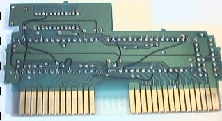 I chose to use AT49F0002 (256K) flashs because I had some in stock. Nintendo's roms pinout at my flash pinouts differ. I had to cut traces on the pcb and solder some wires. Fortunately, there were just a few differences. Here is the document from which I learned the Nintendo ROMs pinout: NES_ROM_Pinouts.txt. Here is another document in which I found the MMC1 pinout: rom.txt
The nes CPU can only address 16 bits, which means 65536 bytes of memory. The memory space is split in two halves, the first 32K are for RAM and IO, the second 32K is mapped to the cartridge ROM.
The PPU have similar limitations.
The allow the use of more memory, supplemental chips are required in the cartridge. Those are named mappers and make bank switching possible. With bank switching, it is possible to point an address range (from the CPU point of view) to various areas in the ROM. eg: Address range $C000-$FFFF which normally points to the range $4000-7FFF in ROM could point to $8000-$C000 instead. This is transparent from the CPU point of view. (except the actual operation of switching bank).
Many different mapper chips exists, and some mappers are very complex. The mapper present in my cartridge is a MMC1 by Nintendo. Here is some documentation about this mapper: mmc1.txt.
Since I wanted to play Bubble Bobble and this game uses MMC1, I chose to use the Motor City Patrol cartridge which also uses the MMC1.
In the cartridge, there is also a protection chip (CIC). The CIC chip communicates with the CIC chip inside the NES. If the communication is successful, the NES's CIC chip stops resetting the NES at 1hz and the game can run. I just left the chip were it was.
 I chose to use AT49F0002 (256K) flashs because I had some in stock. Nintendo's roms pinout at my flash pinouts differ. I had to cut traces on the pcb and solder some wires. Fortunately, there were just a few differences. Here is the document from which I learned the Nintendo ROMs pinout: NES_ROM_Pinouts.txt. Here is another document in which I found the MMC1 pinout: rom.txt
Software
On the internet, NES roms are usually distributed in .nes format. A .nes file contains data from the 2 cartridge roms (PRG and CHR) and a header to specify which mapper is used, the type of mirroring, and the roms sizes. I needed a tool to extract the 2 roms that would work on Linux so I coded my own. (I have not extensively searched).
I have coded 3 simple tools: readnes, nesgg et patchnes.
C source code: nesutils-1.0.tar.gz
C source code + DOS Executables: nesutils-1.0.rar
Update! (October 2011) : Kevin Selwyn wrote a PHP port of readnes: http://www.kevinselwyn.com/ReadNES/
Addresses are displayed as seen by the NES cpu. Shift them right by one to obtain rom addresses.
6 letter codes simply replace a byte at a given address.
8 letters codes replaces a byte at a given address only if the value contained at the same address is equal to the value specified in the game genie code. This prevents the game genie from replacing values that should not be changed. (eg: with bank switching, a NES CPU address does not always represent the same address in ROM).
Example:
Here is a file explaining how NES game genie codes are encoded: nesgg.txt
This will work 100% reliably mapperless roms.
On MMC1 roms, there is a small chance that the wrong value will be changed. That's because I cannot know in advance wether the game will use 32K or 16K bank switching, and I cannot know where the banks will be used (high or low rom). I assume the game uses 16Kb banks and that each bank will be used at High and low locations. Doing so increases odds of replacing the right value at the right address.
I have applied a few codes to Bubble Bubble (MMC1) and it seems to work ok.
Example:
I have coded 3 simple tools: readnes, nesgg et patchnes.
C source code: nesutils-1.0.tar.gz
C source code + DOS Executables: nesutils-1.0.rar
readnes:
./readnes rom.nes [num repeats prg] [num repeats chr]
readnes reads the .nes header, prints the mapper used, prints the type of mirroring, prints the number of prg and chr banks and generates 2 files. One file containing the PRG rom data and another file containing the CHR data.
The content of the PRG or CHR rom can be output more than one time to the PRG or CHR file. This has been useful for me when I had a 128K game to put in a 256K cartridge. Bacause of the way the MMC1 was used, the A14 address line was changing and at times unprogrammed data was read. After repeating the same data 2 times in PRG rom, the state of the A14 line did not matter anymore.
Example:$ ./readnes BUBBLE.NES 2 1 File length :262288 Bytes NES PRG: 08 CHR: 10 MAPPER: 11 44 Nintendo MMC1 Flags: 01 V PRG 8 pages of 16kb (131072 bytes) CHR 16 pages of 8kb (131072 bytes) End at 262160 Remaining bytes: 128 BUBBLE BOBBLE From MINDRAPE and EFX Writing BUBBLE.prg . Writing BUBBLE.chr ..All is left to do after that is too write the .prg and .chr into Flash/ROM.
Update! (October 2011) : Kevin Selwyn wrote a PHP port of readnes: http://www.kevinselwyn.com/ReadNES/
nesgg
Nesgg takes one or many NES game genie codes (6 or 8 letters) from the command line and displays what they mean.Addresses are displayed as seen by the NES cpu. Shift them right by one to obtain rom addresses.
6 letter codes simply replace a byte at a given address.
8 letters codes replaces a byte at a given address only if the value contained at the same address is equal to the value specified in the game genie code. This prevents the game genie from replacing values that should not be changed. (eg: with bank switching, a NES CPU address does not always represent the same address in ROM).
$ ./nesgg PAUKEZLA TAUKEZLA PAUKEZLE
PAUKEZLA: Value: $01  Compare Value: $03  Address: $9470
TAUKEZLA: Value: $06  Compare Value: $03  Address: $9470
PAUKEZLE: Value: $09  Compare Value: $03  Address: $9470
The 3 codes above are for Bubble Bobble. They change the initial number of lives (1, 6 or 9). It is clear that the byte at address $9470 reprents the initial number of lives.
Here is a file explaining how NES game genie codes are encoded: nesgg.txt
patchnes
patchnes applies one or many NES game genie codes to a .NES rom (no mapper or MMC1 only).This will work 100% reliably mapperless roms.
On MMC1 roms, there is a small chance that the wrong value will be changed. That's because I cannot know in advance wether the game will use 32K or 16K bank switching, and I cannot know where the banks will be used (high or low rom). I assume the game uses 16Kb banks and that each bank will be used at High and low locations. Doing so increases odds of replacing the right value at the right address.
I have applied a few codes to Bubble Bubble (MMC1) and it seems to work ok.
Example:
$ ./patchnes BUBBLE.NES PAUKEZLE
Working on rom BUBBLE.NES
Applying 8 letters code 'PAUKEZLE'
Not replacing $11 by 09 at address $9470 because it is not $03
Not replacing $02 by 09 at address $D470 because it is not $03
Not replacing $C4 by 09 at address $11470 because it is not $03
Not replacing $F1 by 09 at address $15470 because it is not $03
Not replacing $A9 by 09 at address $19470 because it is not $03
Not replacing $4C by 09 at address $1D470 because it is not $03
Replaced $03 by $09 at address $21470
Not replacing $FC by 09 at address $25470 because it is not $03
Programming
To program the flashs, I use an old universal programmer from xeltek. You can buy an universal programmer from ebay for approximately 50$ US. You may also build your own programmer since the flash datasheet explain how to program them.
Pictures
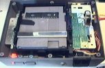
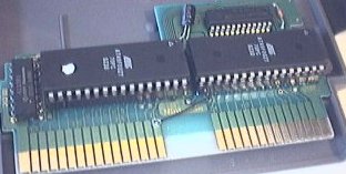 Here we can see the SL-ROM-6 pcb from the Motor City Patrol cartridge. I replaced the roms by two 32 pin sockets. I modified the PCB so the sockets would accept the pinout of the AT49F002 flash roms I use.
It's not easy to see in this picture, but the chips really are in sockets.
Here are some pictures of my cartridge programmed and working:
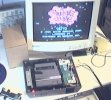
Note: This NES does not have a VGA output. I'm using a video capture card.
Improvements
 A few days later, I realized that I could put two 128Kb games in my 256Kb flash chips. Selecting which game(or bank) to use is as simple as putting a high or low level on the most significant address bit (Right switch). To keep support for 256Kb games, I simply connect the signal from the mapper to the most significant bit, as it was before. (Left switch).
I had to cut more tracks to redirect the signals. Here is a picture of the wiring:

Links
The best NES information site I've found: http://nesdev.parodius.com/
NES roms pinout: NES_ROM_Pinouts.txt
Catridge pinout and mappers pinout: rom.txt
Nintendo's MMC1 mapper information: mmc1.txt
How game genie codes are encoded: nesgg.txt
AT49F002 Flash roms datasheet: doc1017.pdf
NES roms pinout: NES_ROM_Pinouts.txt
Catridge pinout and mappers pinout: rom.txt
Nintendo's MMC1 mapper information: mmc1.txt
How game genie codes are encoded: nesgg.txt
AT49F002 Flash roms datasheet: doc1017.pdf
Disclaimer
I cannot be held responsible for any damages that could occur to you or your equipment while following the procedures present on this page. Also, I GIVE ABSOLUTELY NO WARRANTY on the correctness and usability of the informations on this page. Please note, however, that the procedures above have worked in my case without any damages or problems.
Now you cannot say that I did not warn you :)
Now you cannot say that I did not warn you :)

0 comentarios:
Publicar un comentario